Archive for the ‘Soldering Supplies’ Category

Flux Test Kits, what do they do?

Thursday, August 27th, 2015

Test kits are acid titration kits. As solvent evaporates, the acids in the flux become more and more concentrated. The kit is used to determine the acid number of the flux. The test is a simple drop test with an indicator for the endpoint (similar to a swimming pool test). You count the drops and then go to a chart. From the chart you determine how much thinner to add to bring the acid number back down to spec. Traditionally flux control is maintained by measuring the density of the flux and adding thinner as the flux thickens. This is a good method for fluxes with high solids contents. A slight change in density corresponds to a small change in the flux. The no-clean fluxes have low solids percents (typically 2 or 3 %) so a small change in the flux density could reflect the change in solids of 25-30%. This would put the acid level unacceptably high. The test kits are more accurate than using density measurements as a way to monitor the flux.

Source: Kester Solder Co.

Are Kester “44” rosin residues harmful to an assembly?

Thursday, August 27th, 2015

The “44” flux residues are non-conductive and non-corrosive. Residue removal would normally be for cosmetic reasons. If the assembly is in a heated environment and sees temperatures of over 160°F the flux residues will re-melt. When liquid (at high temperatures) the residues are conductive.

Do rosin flux residues need to be removed?

Thursday, August 27th, 2015

Rosin flux residues are non-conductive and non-corrosive. Under normal circumstances they do not have to be removed from a printed circuit assembly. Rosin residue removal would be for cosmetic considerations. In an environment where the working temperature of the assembly will exceed 200°F the rosin residues will melt and become conductive, in these situations flux removal is required.

Source: Kester Solder

Electronics Assembly

Friday, August 21st, 2015

Rework and Touch-Up

Friday, August 21st, 2015

Indium Corporation manufactures a variety of materials for PCB rework, repair, and touch up, including flux-cored wire, liquid rework fluxes, and TACFluxes®.

Flux Cored Wire

Pb-Free SAC wireIndium Corporation has developed a range of flux-cored wire solutions to meet the needs of virtually every electronic assembly and rework operation from no-clean flux-cored wire for circuit board assembly to activated flux-cored wire for non-sensitive electronics and electrical applications.

No-clean fluxes include:

  • CW-807 halogen free for high reliability assemblies
  • CW-807M, which has a small addition of halogen activator for more difficult to solder assemblies
  • CW-807H for high temperature alloys
  • CW-501 is rosin (colophony) free and shows exceptional soldering on a wide range of assemblies
  • CW-802 is recommended only when no halogen is a must and the process is well-controlled

Activated fluxes include:

  • CW-201, a traditional RA type flux as defined by the legacy Mil-Spec QQ-S-571
  • CW-207 formulated using a blend of heat stable clear rosins
  • CW-209, which has twice the amount of halogen activator as CW-207
  • CW-501, rosin (colophony) free and has exceptionally effective soldering on a wide range of assemblies

Liquid Rework Fluxes

Flux PensLiquid rework fluxes are packaged in convenient pen dispensers, providing the optimal fluxing with no waste. Flux pens utilize a spring-loaded applicator tip to deliver a controlled amount of flux to the work surface. The user friendly pin-point application is deal for touch-up and light assembly work. Liquid fluxes include:

  • FP-500, a halogen-free flux that is compatible with both SnPb and Pb-free assemblies
  • NC-771, a halogen-free, low-residue, all-purpose flux that passes the SIR test in the un-reflowed state
  • FP-300, a water-soluble flux that is compatible with both SnPb and Pb-free assemblies

TACFluxes®

TACFluxTACFluxes® have a variety of uses including rework and repair of various electronics assemblies and components, SMT component attach (including BGAs and flip-chips), BGA ball attach, preform soldering, and virtually any application where flux is required. Indium Corporation manufactures a complete line of TACFlux®, which include no-clean, water-wash, and RMA-based fluxes.

Some of the most common TACFluxes® include:

  • TacFlux 089: no-clean flux for Pb-free alloys
  • TacFlux 089HF: a halogen-free, no-clean flux for Pb-free alloys
  • TacFlux 025: a water-soluble flux for Pb-free and SnPb alloys
  • TacFlux 020B: a halogen-free, no-clean flux for Pb-free alloy

Source: Indium Corporation, Clinton, NY

Low Temperature Alloy Solders

Friday, August 21st, 2015

Low temperature alloys, which typically contain indium or bismuth, melt at temperatures less than 180°C. These low-melting alloys are required for a wide variety of applications, including:

  1. Step soldering involving temperature sensitive components
  2. Soldering to molded interconnect device (MID) plastics
  3. Fusible alloys/fuse applications
  4. Mercury replacement
  5. Thermal and electrical conductivity

Step Soldering Involving Temperature Sensitive Components

Step soldering is the process of attaching components to a substrate in a series of steps where each step in the soldering process uses a lower reflow temperature than the step before it. Standard components are attached first and then temperature sensitive components (like LEDs) are done last. These temperature sensitive components reflow at temperatures less than 180°C.

Soldering To MID Plastics

Molded interconnect device (MID) plastics have been around for many years, but are becoming more popular in product design. MID plastics, which are formed into 3D shapes to increase the functionality and reduce overall weight of each product, are important in automotive and medical applications.

Fusible Alloys/Fuse Applications

Fusible alloys are valued for their relatively low-temperature melting point precision, as well as for their physical properties at room temperature.

Fusible alloys can be used for:

  • Fuses
  • Tube bending
  • Lens blocking
  • Wax pattern dies
  • Potting molds
  • Punch anchoring

Properties

Property Indalloy
117 158 160-190 217-440 255 281
Melting Point or Range Deg/F 117 158 160-190 217-440 255 281
Weight lbs/in3 .32 .339 .341 .343 .380 .315
Tensile Strength lbs/in2 5,400 5,990 5,400 13,000 6,400 8,000
Brinell Hardness No. 12 9.2 9 .19 10.2 22
Maximum Load
30 sec lbs/in2
10,000 9,000 16,000 8,000 15,000
Safe Load Sustained 300 300 300 300 500
Conductivity (Electrical) Compared with Pure Copper 3.34% 4.17% 4.27% 2.57% 1.75% 5.00%
Cumulative Growth and Shrinkage Time after Casting
2 min. +.0005 +.0025 -.0004 +.0008 -.0008 +.0007
6 min. +.0002 +.0027 -.0007 +.0014 -.0011 +.0007
30 min. .0000 +.0045 -.0009 +.0047 -.0010 +.0006
1 hr. -.0001 +.0051 .0000 +.0048 -.0008 +.0006
2 hr. -.0002 +.0051 +.0016 +.0048 -.0004 +.0006
5 hr. -.0002 +.0051 +.0018 +.0049 .0000 +.0005
500 hr. -.0002 +.0057 +.0025 +.0061 +.0022 +.0005

Mercury Replacement

Indium Corporation manufactures several alloys that have very low-melting points. These liquid-at-room-temperature alloys are finding increased uses in various applications as a replacement for the more toxic mercury. In addition, the vapor pressures of these alloys are substantially lower than mercury.

Thermal and Electrical Conductivity

Alloy systems that are liquid at room temperature have a high degree of thermal conductivity, far superior than ordinary non-metallic liquids. This allows for the use of these materials in specific heat-conducting applications, such as the heat dissipation of sensitive components during operation, machining, and/or manufacturing.

Other advantages of these liquid alloy systems are their inherent high densities and electrical conductivities. Typical applications for these materials include thermostats, switches, barometers, heat transfer systems, and thermal cooling and heating designs.

The table below lists available Indalloy® alloys which are liquid at room temperature.

Indalloy
Number
Liquidus C Solidus C Composition Density
lb/in3
Specific
Gravity
gm/cm3
Thermal
Conductivity
(W/mK)
Electrical
Resistivity
(10-8Ω-m)
46L 7.6 6.5 61.0Ga / 25.0In / 13.0Sn / 1.0Zn 0.2348 6.50 15* 33*
51E 10.7 10.7 66.5Ga / 20.5In / 13.0Sn 0.2348 6.50 16.51 28.91
51 16.3 10.7 62.5Ga / 21.5In / 16.0Sn 0.2348 6.50 16.51 28.91
60 15.7 15.7 75.5Ga / 24.5In 0.2294 6.35 20* 29.42
77 25.0 15.7 95Ga/5In 0.2220 6.15 25* 20*
14 29.78 29.78 100Ga 0.2131 5.904 28.13 14.854
* Estimated

References:

1 Geratherm Medical AG, Safety Data Sheet, 93/112/EC, 20042 Michael D. Dickey, et al., Eutectic Gallium-Indium (EGaIn): A Liquid Metal Alloy for the Formation of Stable Structures in Microchannels at Room Temperature, Advanced Functional Materials, 2008, 18, 1097–11043 C.Y.Ho, et al., Thermal Conductivity of the Elements, Journal of Physical Chemical Reference Data, Vol. 1. No 2, 1972.4 Charles Kittle, Introduction to Solid State Physics, 7th Ed., Wiley and Sons, 1996. 

Packaging for Liquid Metal Alloys 

Liquid metal alloys are shipped in polyethylene bottles.

Storage/Shelf Life for Liquid Metal Alloys

Unopened bottles have a guaranteed shelf life of one year. It is recommended that the volume be replaced with dry argon as the material is removed from the bottle. This will minimize any possibility of oxidation on the surface of the alloy. If the alloy has been stored below its melting point and has solidified, it should be remelted and thoroughly shaken or mixed before use.

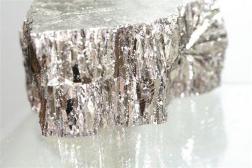
indium-bismuth_low_melting_temp-solder_252bismuth low-temperature melt solder


Source: Carol Gowan, Indium Solder Co.


CircuitWorks Nickel Conductive Pen, CW2000

Wednesday, August 19th, 2015

Circuitworks® Nickel Conductive Pen CW2000

1. What is the Circuitworks® Nickel Conductive Pen and what does it do?
The Circuitworks® Nickel Conductive Pen is the convenient to use pen that makes instant conductive traces and coatings on circuit boards, plastic enclosures, etc. It’s good for linking components, repairing defective traces and making smooth jumpers in cost effective systems. It is also ideal for providing EMI/RFI shielding for electronic components.

2. What’s the difference between the Circuitworks® Conductive Pen and the Circuitworks®
Nickel Conductive Pen?
The Circuitworks® Conductive Pen contains a silver-based compound that is designed for the highest level of conductivity. This product is designed for circuit boards that require the most conductive trace possible. Because of the high silver content, this silver-based Conductive Pen could be cost prohibitive for some repair applications. The Nickel Conductive Pen contains nickel as its conductor. While nickel is not as conductive as silver, it does provide good conductivity for less critical repair work. It is a cost effective alternative to silver-based conductive inks. It does contain the same polymer package as our other conductive pens, so cure times are approximately the same.

3. How electrically conductive is the Circuitworks® Nickel Conductive pen in comparison to
the Circuitworks® Silver Conductive Pen?

The silver-based Circuitworks® Conductive Pen possesses a higher electrical conductivity than the Circuitworks® Nickel Conductive Pen. The conductivity is 0.02 – 0.05 ohms/sq/mil for the Circuitworks® Conductive Pen and 1.0-1.5 ohms/sq/mil for the Circuitworks® Nickel Conductive Pen.

4. What are its features and benefits?

Features:
• Single component system
• Good electrical conductivity
• Fast drying
• Highly adherent to most materials
• Low cost

Benefits:
• Easy application
• Repairs damaged circuits & shielding
• Tack free in 3 to 5 minutes
• Bonds well to circuits and housing components
• Economical solution for conductive requirements

5. How do I use the Circuitworks® Nickel Conductive Pen?
Make sure your board is clean and dry for the best adhesion. We recommend Chemtronics Electro-wash® PX Cleaner/Degreaser to remove any surface contamination that might prevent good material contact. Shake the pen vigorously for 30 seconds to insure proper dispersion of the nickel flakes. Squeeze the pen while pressing down on the surface to begin the flow. Draw the trace along the desired path. It’s best to practice with the pen before attempting detail work.

6. How long does it take the trace to dry?
The Nickel Conductive Pen trace will be tack free in 3 to 5 minutes at room temperature. Electrical conductivity is achieved within 30 minutes. You can heat cure the trace for 10-15 minutes at 80ºC to 100ºC for maximum durability and chemical resistance.

7. Does the Circuitworks® Nickel Conductive Pen require an overcoat to protect it after
it is cured?

The trace created by the Nickel Conductive Pen does need protection after curing. We recommend our Circuitworks® Overcoat Pen for the best results.

8. Can I solder to the trace of the Circuitworks® Nickel Conductive Pen?
The trace created by the Nickel Conductive Pen is not solderable. If your application requires soldering after the trace is cured, try CircuitWorks Silver Conductive Pen. It is solderable at low temperatures.

9. What is the shelf life of the Circuitworks® Nickel Conductive Pen?
Twelve (12) months from the manufacturing date stamped on the container.

CircuitWorks Epoxy Overcoat CW2500

Wednesday, August 19th, 2015

Frequently Asked Questions
Circuitworks® Epoxy Overcoat, CW2500

1. What is an Epoxy Overcoat?
Circuitworks® Epoxy Overcoat is a permanent green coating formulated to protect circuit traces before being exposed to reflow conditions. It is a two component, 100% solids epoxy that is engineered specifically for high temperature resistance, used for electronic circuit and component protection. When properly cured the insulator forms a chemically inert coating that seals out moisture and environmental contaminants, minimizes thermal shock and prevents corrosion, oxidation, and abrasion. The Epoxy Overcoat easily withstands brief exposure to high temperatures found in normal wave and reflow applications.

2. What is the difference between Circuitworks® Overcoat Pen (CW3300G) and Circuitworks® Epoxy Overcoat?
Circuitworks® Overcoat Pen is a one component, acrylic-based system with fair heat resistance and satisfactory chemical
resistance. When subject to reflow conditions this material will quickly degrade. However it does have excellent electrical insulation and good abrasion resistance. Circuitworks® Overcoat Pen is primarily designed for protecting and electrically insulating circuit board traces and components, with an easy to use one component system.

Circuitworks® Epoxy Overcoat is a two component system with outstanding high temperature and chemical resistance. Abrasion
resistance is also excellent for this epoxy system. It’s the best choice for repairing the permanent solder mask/solder resist when the boards will be subject to reflow conditions. It also has outstanding dielectric properties as permanent coating for use on bare metal.

3. What is the mixing ratio?
The mixing ration is the volume of part A needed to mix with part B. This can be critical with some epoxy systems, and can be
difficult to get the exact quantities in the right ratios as 0.96:1.32 is not unusual. This epoxy system was developed to provide
easy mixing ratios, with a very forgiving cure system. The mixing ratio for the Epoxy Overcoat is 1:1, but this ratio is not critical to obtain the best electrical and protective capabilities.

4. What are the features and benefits of the Circuitworks® Epoxy

Features

• High temperature resistance
• Provides a hard, durable protective coating
• Excellent dielectric properties
• Solvent resistant
• Service temperature -55ºF/-48ºC to 600ºF/315ºC
• Meets IPC-7721.2.4.1 requirements

Benefits
• Ideal for pre-reflow solder resist repair
• Prevents corrosion, corrosion, oxidation, degradation and thermal shock
• Electrically insulative coating helps prevent electrical discharge
• Will not be removed by solvent cleaners
• Can be used in many environments
• Perfect as solder resist board repair

5. How is the Circuitworks® Epoxy Overcoat packaged?
The Epoxy Overcoat is packaged in two (one part A and one part B) easy to use syringes that hold approximately six (6) grams of
material. One syringe contains the epoxy, while the other contains the hardener. This allows you to use as little or as much material as you need.

6. What type of customers would use the Circuitworks® Epoxy Overcoat?
Customers involved in the manufacture and the rework/repair of printed circuit boards would use the Circuitworks® Epoxy Overcoat.
This would include those involved in:
• Circuit board manufacturing
• Data communications
• Aerospace industry
• Instrumentation and control manufacturing
• General maintenance repair

7. Can the Circuitworks® Epoxy Overcoat be used as an encapsulant?
Circuitworks® Epoxy Overcoat’s physical properties are very similar to epoxy encapsulants; it will work to encapsulate leads, traces
and small areas that need insulation and protection. However, the small quantity contained in each syringe does not make it an
ideal candidate for encapsulation.

8. Can the Circuitworks® Epoxy Overcoat be used as a conformal coating?
Conformal coatings are applied in thin layers onto printed circuit boards to provide environmental and mechanical protection to
components and circuitry. Even though the Circuitworks® Epoxy Overcoat can provide protection, the higher viscosity and small
quantity contained in each syringe does not make an ideal candidate for performing as a conformal coating.

9. What’s the shelf life of the Epoxy Overcoat?
The shelf life is twelve (12) months from the manufacturing date.

Chemask NA Non-Ammoniated Solder Mask

Wednesday, August 19th, 2015

Frequently Asked Questions
Chemask® NA Non-Ammoniated Solder Mask

1. What is Chemask® NA? What are its features and benefits?
Chemask® NA Non-Ammoniated Solder Masking Agent is a fast curing, peelable temporary spot mask formulated for safe use on
sensitive metals. It contains high-temperature resistant compounds that protect component-free areas during wave soldering.
Chemask® NA may also be used to protect pins, posts, contacts and edge connections in the solder reflow oven or during
conformal coating processes.

• Stable to 550°F (288°C) – withstands lead-free processing temperatures
• Ideally suited for use with gold, copper, nickel, silver and OSP finishes
• Works with both lead-free and tin/lead applications
• Phthalate-free, low toxicity and environmentally safe
• Compatible with all flux types and cleaning solvents
• Dries tack free in 15 minutes (10 mil thick application)
• Can be introduced into the pre-heat oven without being fully cured
• Removes easily by hand and leaves no residue
• Non-contaminating, non-staining and non-corrosive on all surfaces
• RoHS compliant

2. How does the new Chemask® NA compare to the latex peelable mask Chemask® CM8?
Chemask® NA is also a peelable mask and works as well as Chemask® CM8. The primary differences are that Chemask® NA does
not contain ammonia, and is therefore compatible with lead-free board finishes such as immersion silver, immersion gold, nickel,
lead-free HASL and Entek. Chemask® NA can also be used on standard tin/lead board finishes, including bare copper. Chemask®
NA will also withstand hotter processing temperatures and longer cycling times than any other mask on the market today.
Chemask® NA is not as elastic as Chemask® CM8, which tends not to be a problem with most electronic applications. For other
applications, it can be used successfully on a variety of non-porous surfaces.

3. How do I use Chemask® NA?
When applying the mask by hand using 8 oz. squeeze bottle, insure that all areas of the pre-tinned hole or pad are evenly covered
on the side to be soldered. Automatic dispensing equipment may also be used as appropriate. Chemask® NA can also be applied
using a screen or a stencil. For ease of removal, a minimum thickness of 30 mils is recommended.
Chemask® NA can go straight into the pre-heat oven of a wave soldering machine, or can go into a reflow oven 15 minutes after
application to the PCB. This mask may remain on assemblies for extended periods of time prior to or after processing.
After processing the board, Chemask® NA can be easily peeled off the board by hand or using tweezers.

4. What if I want to apply an extra thick layer of Chemask® NA to the board?
When Chemask® NA is applied in a thick application (> 1/8″), allow extra drying time or oven dry at 250ºF for 30 minutes.

5. If I put Chemask® NA into the pre-heat oven after a short 15 minute cure time, won’t
bubbles form in the mask?

No. Chemask® NA will withstand preheat temperatures without degradation or distortion of the film and will be completely cured by
the end of the processing cycle.

6. Is Chemask® NA completely non-flammable?
Yes. Chemask® NA is non-flammable and contains no flammable components.

7. Is Chemask® NA safe to use?
Yes. Chemask® NA has no strong odors, is non-toxic and, unlike competitors’ products, does not contain phthalates.

8. Is Chemask® NA RoHS compliant?
Yes. RoHS certificates are available on the Chemtronics website www.Chemtronics.com.

9. Is Chemask® NA environmentally friendly?
Yes. Chemask® NA contains no VOC’s or other harmful volatile components. After it has been cured, Chemask® NA can generally
be disposed of without any worries about hazardous waste generation.

10. How can I tell if the product I am using is Chemask® or Chemask® NA?
Chemask® NA is tinted green while the other peelable Chemask® products (Chemask®, Chemask® HV and Chemask® Lead-Free)
are pink.
11. What is the shelf life of Chemask® NA?
The shelf life is three (3) years from the manufacturing date stamped on the container.

12. What type of companies would be interested in these products?
The primary customers that use temporary solder masks are electronics manufacturers, including OEM and contract
manufacturing companies.

13. How is the product packaged?
Chemask® NA is available in two sizes:
• CNA8 8 oz. squeeze bottle packaged in 24 per case
• CNA1 1 gallon

Source: ITW Chemtronics

Lead Free Soder-Wick

Tuesday, August 18th, 2015

Soder-Wick® Lead-Free
1) What exactly is Soder-Wick® Lead-Free SD?
Soder-Wick® Lead-Free SD is a new desoldering braid that has been engineered specifically for optimal removal of lead-free solders, which have a much higher melting point than tin/lead solders. However, it is also effective at removing current tin/lead solders. The SD designation means that the desoldering braid is wound on a static dissipative bobbin to protect the board being reworked from a destructive static discharge.

2) What is the difference between the new Soder-Wick Lead-Free SD and other desoldering
braids like the original Soder-Wick® Rosin and Soder-Wick® No Clean?

The innovative weave of Soder-Wick® Lead-Free SD conducts heat more quickly to the solder joint so more heat energy goes where it is needed to melt the higher melting point, lead-free solders. This shortens the time it takes the solder to liquefy and shortens the overall time required to remove solder when using Soder-Wick® Lead-Free SD. Also, since more of the heat is transferred to the solder joint, Soder-Wick® Lead-Free SD alleviates some of the burden on the soldering iron. The quicker heat transfer means that the operator must also work more quickly to prevent overheating of the solder joint, pad or component. Other wick products do not conduct heat to the solder as quickly and place more emphasis on moderating the heat transfer into the joint. One additional benefit is that some users may find that they can use temperatures for lead-free desoldering similar to conventional tin/lead solders when desoldering with Soder-Wick® Lead-Free. This will reduce oxidation and increase soldering iron tip life
compared with much higher temperature applications.

The innovative weave also makes Soder-Wick® Lead-Free smoother than the current Soder-Wick® Desoldering Braid. This is done
to reduce scratching and marring pads.

Soder-Wick® Lead-Free SD employs a ‘no clean’ flux specifically formulated to tolerate the higher temperatures and poorer wetting capability of currently available lead-free solders.

3)Do I have to use Soder-Wick® Lead-Free to remove lead free solders?
No, Soder Wick® Rosin and Soder-Wick® No Clean will also effectively remove lead-free solder but they are not optimized for leadfree
solder removal. They will require
(a) a soldering iron tip that is slightly larger than the joint and desoldering braid,
(b) possibly higher temperatures, which may shorten soldering tip life and
(c) a higher power soldering iron for faster thermal recovery.Some operators may actually prefer the original Soder-Wick® products and are more comfortable adapting their technique and equipment to lead-free solders, rather than changing to the new Soder-Wick® Lead-Free.

4) Does Soder-Wick® Lead-Free remove lead containing solders effectively?
Yes, Soder-Wick® Lead-Free effectively removes conventional lead containing solders. However, operators accustomed to the original Soder-Wick® may find that the braid heats-up more quickly and must adapt their technique.